| 积层陶瓷电容 (MLCC) |
MLCC 应用注意事项
|
Storage
1.The chip capacitors shall be packaged in carrier tapes or bulk cases.
2.Keep storage place temperatures from +5℃ to +35℃, humidity from 45 to 70% RH.
3.The storage atmosphere must be free of gas containing sulfur and chlorine. Also, avoid exposing the product to saline moisture. If the product is exposed to such atmospheres, the terminations will oxidize and solderability will be affected.
4.The solderability is assured for 12 months from our final inspection date if the above storage condition is followed. |
Circuit Design
1.Once application and assembly environments have been checked, the capacitor may be used in conformance with the rating and performance, which are provided in both the catalog and the specifications. Exceeding the specifications listed may result in inferior performance. It may also cause a short, open, smoking, or flaming to occur, etc.
2.Please use the capacitors in conformance with the operating temperature provided in both the catalog and the specifications. Be especially cautious not to exceed the maximum temperature. In the situation the maximum temperature set forth in both the catalog and specifications is exceeded, the capacitor’s insulation resistance may deteriorate, power may suddenly surge and short-circuit may occur. The loss of capacitance will occur, and may self-heat due to equivalent series resistance when alternating electric current is passed through. As this effect becomes critical in high frequency circuits, please exercise with caution. When using the capacitor in a (self-heating) circuit, please make sure the surface of the capacitor remains under the maximum temperature for usage. Also, please make certain temperature rise remain below 20℃.
3.Please keep voltage under the rated voltage, which is applied to the capacitor. Also, please make certain the peak voltage remains below the rated voltage when AC voltage is super-imposed to the DC voltage. In the situation where AC or pulse voltage is employed, ensure average peak voltage does not exceed the rated voltage. Exceeding the rated voltage provided in both catalog and specifications may lead to defective withstanding voltage or, in worse case situations, may cause the capacitor to burn out.
4.It’s is a common phenomenon of high-dielectric products to have a deteriorated amount of static electricity due to the application of DC voltage. |
Handling
Chip capacitors should be handled with care to avoid contamination or damage. The use of vacuum pick-up or plastic tweezers is recommended for manual placement. Tape and reeled packages are suitable for automatic pick and placement machine. |
Flux
1.An excessive amount of flux or too rapid temperature rise can causes solvent burst, solder can generate a large quantity of gas. The gas can spreads small solder particles to cause solder balling effect or bridging problem.
2.Flux containing too high of a percentage of halide may cause corrosion of termination unless sufficient cleaning is applied.
3.Use rosin-type flux. Highly acidic flux (halide content less than 0.2wt%) is not recommended.
4.The water soluble flux causes deteriorated insulation resistance between outer terminations unless sufficiently cleaned. |
Component Spacing
For wave soldering components, the spacing must be sufficient far apart to prevent bridging or shadowing. This is not so important for reflow process but enough space for rework should be considered. The suggested spacing for reflow soldering and wave soldering is 0.5mm and 1.0mm, respectively. |
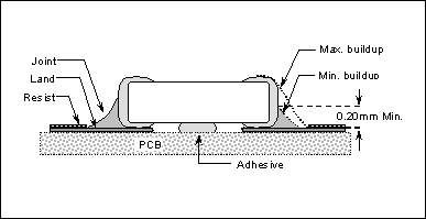
Solder Fillet
Too much solder amount may increase solder stress and cause crack risk. Insufficient solder amount may reduce adhesive strength and cause parts falling off PCB. When soldering, confirm that the solder is placed over 0.2mm of the surface of the terminations.
 |
|
Recommended Pad Dimensions
When mounting the capacitor to substrate, it’s important to consider that the amount of solder (size of fillet) used has a direct effect upon the capacitor once it’s mounted.
1.The greater the amount of solder, the greater the stress to the elements, as this may cause the substrate to break or crack.
2.In the situation where two or more devices are mounted onto a common land, separate the device into exclusive pads by using soldering resist.
3.Land width equal to or less than component. It is permissible to reduce land width to 80% of component width. 3.Land width equal to or less than component. It is permissible to reduce land width to 80% of component width.
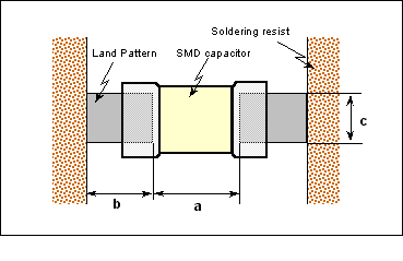
| Size mm(EIA) |
L x W(mm) |
a(mm) |
b(mm) |
c(mm) |
| 0603(0201) |
0.6*0.3 |
0.15 to
0.35 |
0.2 to
0.3 |
0.25 to
0.3 |
| 1005(0402) |
1.0*0.5 |
0.3 to
0.5 |
0.35 to
0.45 |
0.4 to
0.5 |
| 1608(0603) |
1.6*0.8 |
0.7 to
1.0 |
0.6 to
0.8 |
0.7 to
0.8 |
| 2012(0805) |
2.0*1.25 |
1.0 to
1.3 |
0.7 to
0.9 |
1.0 to
1.2 |
| 3216(1206) |
3.2*1.6 |
2.1 to
2.5 |
1.0 to
1.2 |
1.3 to
1.6 |
| 3225(1210) |
3.2*2.5 |
2.1 to
2.5 |
1.0 to
1.2 |
2.0 to
2.5 |
| 4520(1808) |
4.5*2.0 |
3.2 to
3.8 |
1.2 to
1.4 |
1.7 to
2.0 |
| 4532(1812) |
4.5*3.2 |
3.2 to
3.8 |
1.2 to
1.4 |
2.7 to
3.2 |
|
|
Resin Mold
If a large amount of resin is used for molding the chip, cracks may occur due to contraction stress during curing. To avoid such cracks, use a low shrinkage resin. The insulation resistance of the chip will degrade due to moisture absorption. Use a low moisture absorption resin. Check carefully that the resin does not generate a decomposition gas or reaction gas during the curing process or during normal storage. Such gases may crack the chip capacitor or damage the device itself.
|
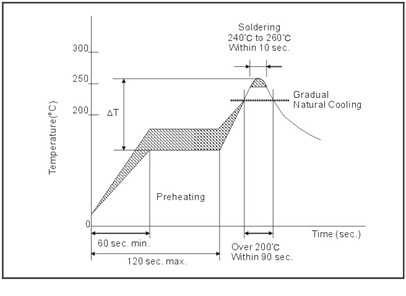
Soldering Profile for SMT Process with SnPb Solder Paste
Reflow Soldering
The difference between solder and chip surface should be controlled as following table. The rate of preheat should not exceed 4℃/sec and a target of 2℃/sec is preferred.
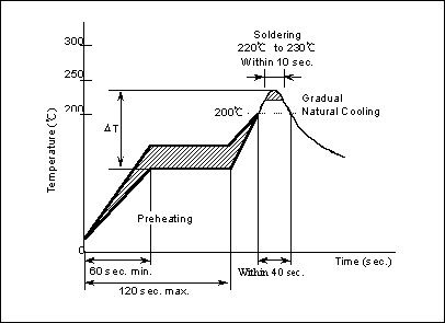
| Chip Size |
3216 abd smaller |
3225 and above |
| Preheating |
△T≦150℃ |
△T≦130℃ |
|
Wave Soldering
| Chip Size |
3216 abd smaller |
3225 and above |
| Preheating |
△T≦150℃ |
- |
|
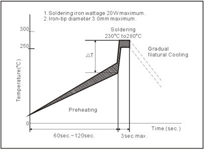
Soldering Iron
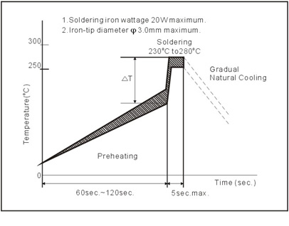
| Chip Size |
3216 abd
smaller |
3225 and
above |
| Preheating |
△T≦190℃ |
△T≦130℃ |
|
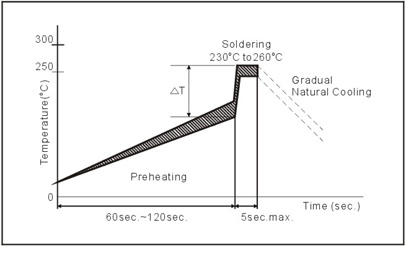
Reflow Soldering for Lead free Termination
The difference between solder and chip surface should be controlled as following table.
The rate of preheat should not exceed 4℃/sec and a target of 2℃/sec is preferred.
| Chip Size |
3216 abd
smaller |
3225 and
above |
| Preheating |
△T≦150℃ |
△T≦130℃ |
|
Flow Soldering for Lead free Termination

| Chip Size |
3216 abd
smaller |
3225 and
above |
| Preheating |
△T≦150℃ |
- |
|
Soldering Iron
| Chip Size |
3216 abd
smaller |
3225 and
above |
| Preheating |
△T≦150℃ |
△T≦130℃ |
|
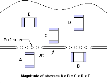
Chip Layout and Breaking PCB
1.To layout the SMD capacitors for reducing bend stress from board deflection of PCB. The following are examples of good and bad layout.

2.When breaking PCB, the layout should be noted that the mechanical stresses are depending on the position of capacitors. The following example shows recommendation for better design.
 |
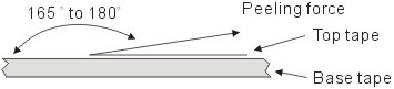
Reeling off Force
Peeling off force: 0.1N to 1.0N in the direction shown below.
The peeling speed: 300+/-10 mm/min
1. The taped tape on reel is wound clockwise. The sprocket holes are to the right as the tape is pulled toward the user.
2. There are minimum 150 mm as the leader and minimum 40 mm empty tapes as the tall is attached to the end of the tape.
|

