| |
Item |
Specification |
Test Method |
| Temp. compensating type |
High dielectric constant type |
| 1 |
Operating Temperature Range |
Np0: -55 to 125 degree C |
X7R: -55 to 125 degree C
X5R: -55 to 85 degree C
Y5V: -30 to 85 degree C
|
|
| 2 |
Rated Voltage |
4VDC, 6.3VDC, 10VDC, 16VDC, 25VDC, 35VDC, 50VDC, 100VDC, 200VDC, 250VDC, 500VDC, 630VDC, 1000VDC, 2000VDC, 3000VDC |
The rated voltage is defined as the maximum voltage, which may be applied continuously to the capacitor. |
| 3 |
Appearance |
No defects or abnormalities. |
Visual inspection |
| 4 |
Dimensions |
Within the specified dimension. |
Using calipers |
| 5 |
Dielectric Strength |
No defects or abnormalities. |
No failure shall be observed when 250%* of the rated voltage ( 150% for 500V, 120% for above 1KV ) is applied between the terminations for 1 to 5 seconds. The charge and discharge current is less than 50mA. |
| 6 |
Insulation Resistance(I.R.) |
| Rated Voltage: <500V |
To apply rated voltage. |
I.R. ≧10G or RiCR≧500Ω-F
(whichever is smaller)
|
| Rated Voltage: ≧500V |
To apply 500V. |
|
The insulation resistance shall be measured with a DC voltage not exceeding the rated voltage at 25℃ and 75%RH max, and within 1 minute of charging. |
| 7 |
Capacitance |
Within the specified tolerance
* X7R, X5R and Y5V at 1000 hours
|
The capacitance / D.F. shall be measured at 25°C at the frequency and voltage shown in the tables.
| Item |
Class I
C≦1,000pF |
Class II
>1,000pF |
* Class II |
| Frequency |
1.0±0.2MHz |
1.0±0.2KHz |
1.0±0.2KHz |
| Voltage |
1.0±0.2Vrms |
1.0±0.2Vrms |
1.0±0.2Vrms |
* For capacitance>10uF, the measure frequency is 120Hz+/-10% and voltage 0.5+/-1Vrms. |
| 8 |
Q/Dissipation Factor(D.F.) |
NP0:
If C≦30pF, DF≦1/(400+20C), C in pF
If C >30pF, DF≦0.1%.
|
I. X5R, X7R:
See X5R,X7R DF table
II. Y5V:
See Y5V DF table.
|
| 9 |
Capacitance Temperature Characteristics |
Capacitance change
NPO within 0±30ppm/℃ under operating temperature range.
|
Capacitance change
X7R/X5R within ±15%
Y5V: -82 to + 22% |
1. Temperature compensating type:
The capacitance value at 25℃ and 85℃ shall be measured and calculated from the formula given below.
T.C.=(C85-C25)/C25*△T*106(PPM/℃)
2.High dielectric constant type:
The ranges of capacitance change compared with the 25℃ value over the temperature ranges shall be within the specified ranges. |
| 10 |
Termination Strength |
No removal of the terminations or marking defect. |
Apply a parallel force of 5N to a PCB mounted sample for 10±1sec. *2N for 0603 (EIA 0201). |
| 11 |
Deflection(Bending Strength) |
No cracking or marking defects shall occur at 1mm deflection.
Capacitance change:
NPO: within ±5% or ± 0.5pF. (whichever is larger)
X7R, X5R:within ±12.5%
Y5V: within ±20%
|
Solder the capacitor to the test jig(glass epoxy boards) shown in Fig.a using a eutectic solder(then let sit for 48±4 hours for X7R X5R and Y5V).
Then apply a force in the direction shown in Fig.b. The soldering shall be done with the reflow method and shall uniform and free of defects such as heat shock. |
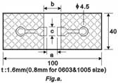
| Size |
a |
b |
c |
| 0603 |
0.3 |
0.9 |
0.3 |
| 1005 |
0.4 |
1.5 |
0.5 |
| 1608 |
1.0 |
3.0 |
1.2 |
| 2012 |
1.2 |
4.0 |
1.65 |
| 3216 |
2.2 |
5.0 |
2.0 |
| 4520 |
3.5 |
7.0 |
2.5 |
| 4532 |
3.5 |
7.0 |
3.7 |
|
 |
|
| 12 |
Solderability of Termination |
90% of the terminations are to be soldered evenly and continuously. |
Immerse the test capacitor into a methanol solution containing rosin for 3 to 5 seconds, preheat it 150 to 180℃ for 2 to 3 minutes and immerse it into Sn-3.0Ag-0.5Cu solder of 245 ± 5℃ for 3±1seconds. |
| 13 |
Resistance to Soldering Heat |
Appearance |
No marking defects |
*Preheat the capacitor at 120 to 150℃ for 1 minute.
Immerse the capacitor in a SAC305(Sn96.5Ag3.0Cu0.5) ?solder solution at 270±5℃ for 10±1 seconds. Let sit at room temperature for 24±2 hours (temperature compensating type) or 48±4 hours (high dielectric constant type), then measure.
*Preheat at 150 to 200℃ for size ≧ 3216.
*High dielectric constant type: Initial measurement: perform a heat treatment at 150+/-10℃ for one hour and then let sit for 48±4hours at room temperature. Perform the initial measurement. |
| Cap. Change |
NP0 within ±2.5% or 0.25pF ( whichever is larger ) |
X7R/X5R within ±7.5%
Y5V within ±20%
|
| Q/D.F. |
If C≦30pF, DF≦1/(400+20C)
If C >30pF, DF≦0.1%
|
To satisfy the specified initial spec. |
| I.R. |
I.R.≧10,000MW or RiCR≧500W-F.
(whichever is smaller)
|
I.R.≧10,000MW or RiCR≧500W-F.
(whichever is smaller)
|
| 14 |
Temperature cycle(Thermal shock) |
Appearance |
No marking defects |
Solder the capacitor to supporting jig (glass epoxy board) and perform the five cycles according to the four heat treatments listed in the following table. Let sit for 24±2hrs at room temperature, then measure.
Step 1: Minimum operating temperature
|
30±3min |
| Step 2: Room temperature |
2~3min |
| Step 3: Maximum operating temperature |
30±3min |
| Step 4: Room temperature |
2~3min |
*High dielectric constant type: Initial measurement: perform a heat treatment at 150+/-10℃ for an hour and then let sit for 48±4 hours at room temp. Perform the initial measurement. |
| Cap. Change |
NP0 within ±2.5% or 0.25pF ( whichever is larger ) |
X7R/X5R within ±7.5%
Y5V within ±20%
|
| Q/D.F. |
If C≦30pF, DF≦1/(400+20C)
If C >30pF, DF≦0.1%
|
To satisfy the specified initial spec. |
| I.R. |
I.R.≧10,000MW or RiCR≧500W-F.
(whichever is smaller)
|
I.R.≧10,000MW or RiCR≧500W-F.
(whichever is smaller)
|
| 15 |
Humidity load |
Appearance |
No marking defects |
Apply the rated voltage at 40±2℃ and 90 to 95% humidity for 500±12 hours. Remove and let sit for 24±2 hours (temperature compensating type) or 48±4 hours (high dielectric constant type) at room temperature, then measure.
The charge / discharge current is less than 50mA.
Pre-treatment: Apply the rated DC voltage for 1 hr at 40±2℃ and 90 to 95% humidity. Remove and let sit for 48±4 hours, then perform the initial measurement.
Initial measurement for high dielectric type. Apply the rated DC voltage for 1 hour at 40±2℃. Remove and let sit for 48±4 hours at room temperature then perform initial measurement. |
| Cap. Change |
NP0 within ±7.5% or 0.75pF
( whichever is larger ) |
X7R/X5R within ±12.5%
Y5V within ±30%
|
| Q/D.F. |
If>30pF, DF≦0.5%
If C≦30pF,D≦1/(100+10xC/3) C in pF
|
X7R 200% max of initial spec.
Y5V 150% max of initial spec.
X5R 200% max of initial spec.
|
| I.R. |
I.R.≧500MW or RiCR≧25W-F.
(whichever is smaller)
|
I.R.≧500MW or RiCR≧25W-F.
(whichever is smaller)
|
| 16 |
High temperature load life test |
Appearance |
No marking defects |
Apply 200%(150% for≧500V; 120% for≧1000V) of the rated voltage for 1000±12 hours at the maximum operating temperature ± 3℃. Let sit for 24± 2 hours (temperature compensating type) or 48±4 hours (high dielectric constant type) at room temperature, then measure.
The charge/discharge current is less than 50mA.
P.S.: Please refer to table 1 for items applying 150% voltage.
Pre-treatment:
Apply 200%* of the rated voltage for 1 hr at maximum operating temperature ±3℃. Remove and let sit for 48±4 hours, then perform the initial measurement.
* 150% for high dielectric constant type≧500V.
* 120% for voltage ≧ 1000V.
* some of the parts are applicable in rated voltage *1.5. please
refer to table 1
|
| Cap. Change |
NP0 within±7.5% or 0.75pF
(whichever is large) |
X7R/X5R within±12.5%
Y5V within±30% |
| Q/D.F. |
If C>30pF,DF≦0.3%
If 10pF<C≦30pF,DF≦1/(275+5xC/2)
If C≦10pF, DF≦1/(200+10C), C in pF |
X7R 200% max of initial spec.
Y5V 150% max of initial spec.
X5R 200% max of initial spec. |
| I.R. |
More than 1GΩ or RiCR≧50Ω-F
(whichever is less.) |
More than 1GΩ or RiCR≧50Ω-F
(whichever is less.) |

